Misfit-structured materials are the basis for fuel-free Neutrinovoltaic power generation technology
- https://n-n-n.ru
- Dec 28, 2025
- 4 min read
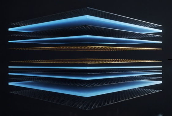
Neutrinovoltaic's fuel-free graphene power generation technology is based on a multilayer nanomaterial made of graphene and doped silicon. This material was developed by scientists at the Neutrino Energy group, led by mathematician Holger Thorsten Schubart, the project's scientific director.

A multilayer nanomaterial is a misfit material. A misfit material (from the English word misfit, meaning "unsuitable" or "inconsistent") is a special class of layered crystalline materials in which individual layers have mismatched crystal lattice parameters (different periods, angles, and symmetries).
Key Features of a Misfit Material
Lattice Mismatch: Layers with different crystal structure parameters are "forced" to align, creating internal stresses and unique interlayer boundaries.
Structural Self-Organization: Despite the mismatch, the system forms a stable heterostructure due to:
elastic deformations of the layers;
the appearance of misfit dislocations;
modulation of the periodicity at the boundaries.
Unusual Physical Properties: Such materials exhibit effects impossible in homogeneous crystals:
superconductivity (in some compounds);
spin-valley polarization (the relationship between electron spin and its position in the Brillouin zone);
anomalous electrical conductivity;
quantum size effects.
Composition example: A typical example is the graphene-silicon compound. Their lattices have different periods, but form a stable heterostructure with charge transfer between the layers.
Difficulties in studying graphene-silicon compounds:
Difficulty in obtaining high-quality single crystals.
Need for precise control of interlayer interfaces.
Difficulty in modeling the electronic structure due to lattice disproportion.
Graphene-silicon materials with a disrupted crystal structure can be called the "superheroes" of materials science. Their "imperfection," that is, the mismatch of their crystal lattices, gives them unique properties sought after in advanced energy technologies, particularly Neutrinovoltaic technology.
A paper on the new method and its application to incommensurate layers has been published in the journal Physical Review Letters. The paper is titled "Unmasking Charge Transfer in the Misfits: ARPES and Ab Initio Prediction of Electronic Structure in Layered Incommensurate Systems without Artificial Strain." Scientists from Cornell University have discovered that in certain complex quantum materials, electrons predominantly remain in their original layers and do not migrate between them. To this end, the researchers developed a new computational technique that allows them to precisely determine where electrons move and where they don't in these multilayer crystals.
We're talking about materials with mismatched crystal lattice parameters, such as nanomaterials used in neutrinovoltaics. In these materials, the lattices of adjacent layers have different periodicities: one layer has a square grid, while the other has a hexagonal grid. The material appears uniform from the outside, but at the atomic level, the layers cannot be perfectly connected. Such structures are of interest for studying unusual quantum phenomena.
It has long been believed that significant energy band shifts in mismatched systems are due to the physical movement of large numbers of electrons from one layer to another. However, research by Cornell scientists has shown that this is not the case. They discovered that chemical bonds at the boundaries between mismatched layers cause a redistribution of electrons within each layer and increase the number of high-energy electrons. However, the actual movement of particles between layers is comparatively small.
Misfit structures have proven to be an excellent platform for testing a new computing method. This approach is based on the principle that electrons in a solid primarily respond to their immediate environment. At the microscopic level, an electron can be thought of as a wave propagating through a crystal. However, in a dense electron system, multiple waves cancel each other out, like ripples on the surface of a crowded pool. As a result, the local environment, rather than the crystal as a whole, is key to the behavior of an individual electron. Research has revealed that the number of high-energy electrons increases in the hexagonal layer, which has traditionally been explained by significant charge transfer from the adjacent layer. However, detailed quantum mechanical calculations by Nejelski revealed that the actual charge transfer was approximately six times weaker than previously assumed. Most electrons simply changed their distribution within the layer, barely escaping beyond its boundaries.
The results of research conducted by Cornell University scientists provide additional insight into the processes occurring in a multilayer nanomaterial developed by engineers and scientists from the Neutrino Energy group. The nanomaterial operates on the basis of quantum excitation, using phonons, plasma exciters, and electrons.
The main advantages of nanostructured materials are manifested in three key aspects:
In this technology, energy transfer is independent of macroscopic gradients. Energy moves through a local flow of momentum and energy, which is ensured by the density of quantized events. These events occur in discrete "portions"—quantum transitions between system states. It is the density of these events that determines the power of the energy flow. This approach eliminates the collective motion of macroscopic objects, significantly reducing macroscopic losses such as friction, thermal conductivity, and energy dissipation in material defects.
High interfacial density implies the maximum number of interfaces between layers per unit volume. In multilayer structures, this increases the area of active surfaces interacting with particles (e.g., neutrinos or nuclei), which facilitates the concentration of energy processes at the nanoscale. Parallel bonds play a key role in this process. Each atomic layer acts as an active element. Neutrino scattering, nuclear interactions, and energy transfer via lattice vibrations occur via planar parallel coupling rather than traditional point coupling. This significantly increases the energy harvesting efficiency per unit volume. The material's unique architecture, which includes a multilayer structure with parallel couplings, significantly improves its energy harvesting capacity.
Coherent propagation of quantized vibration is another important property. Microscopic vibrations, such as phonons and plasmonic excitons, can propagate over long distances in highly conductive two-dimensional materials, including graphene. This enables the integration and amplification of multiple microscopic effects, overcoming the limitations of the low energy of individual events.
Thus, studying microscopic misfit processes in graphene-silicon materials opens up broad possibilities for the industrial implementation of fuel-free Neutrinovoltaic power generation technology.
Authors: Holger Thorsten Schubart, L.K. Rumiantcev


Comments